8-Bit Computer (SAP-1)
Complete SAP-1 computer implementation from Proteus simulation to breadboard and PCB fabrication
Project Overview
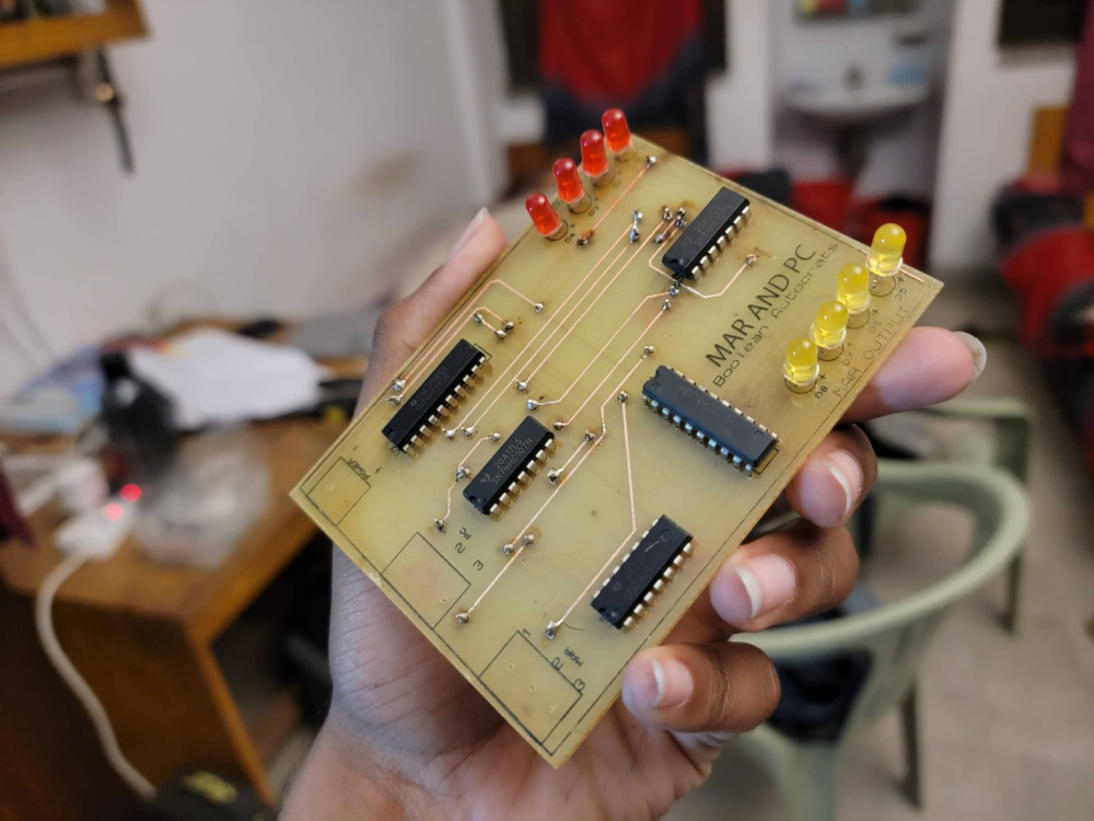
This project focuses on designing and implementing an 8-bit computer based on the SAP-1 (Simple-As-Possible) architecture. The design is developed using the Proteus simulator and later implemented in hardware using PCB boards and commonly available ICs. The goal is to demonstrate the working principle of a basic stored-program computer through modular construction of its key components.
Key Features
- Clock Pulse Generation: Provides the timing signals necessary for synchronization of all modules
- Program Counter: Sequentially generates memory addresses for instruction execution
- Memory & Input Handling: Includes Memory Address Register (MAR), RAM, and input unit for data/instruction management
- Registers: Accumulator, B-register, and Output register for temporary data storage and transfer
- Instruction Handling: Instruction Register and Controller/Sequencer for instruction decoding and execution control
- Arithmetic Operations: ALU supporting addition and subtraction
- Modular Phased Design: Clear separation into Phase A, B, C, and D for systematic implementation
Technical Implementation
The system is divided into four implementation phases:
-
Phase A – Basic Control Units
- Clock Pulse Generator: Generates clock signals for system synchronization
- Program Counter: 4-bit counter (0–15) with enable/reset features
- Memory Address Register (MAR): Stores current address and passes it to memory or bus
-
Phase B – Data Storage Modules
- Registers:
- Accumulator: Holds intermediate ALU results
- B-Register: Secondary operand storage
- Output Register: Displays final results
- RAM: Stores instructions and data for execution
- Registers:
-
Phase C – Control & Instruction Handling
- Instruction Register: Separates opcode and operand during fetch cycle
- Controller/Sequencer: Generates control signals (T-states) for fetch-decode-execute cycles
-
Phase D – Processing Unit
- Arithmetic Logic Unit (ALU): Performs addition and subtraction using inputs from Accumulator and B-register
- Works under Controller/Sequencer signals for proper operation timing
System Architecture
- Control Layer: Clock Pulse Generator, Program Counter, Controller/Sequencer
- Memory Layer: MAR and RAM for instruction/data storage
- Register Layer: Accumulator, B-register, Output register
- Instruction Layer: Instruction Register for opcode/operand separation
- Processing Layer: ALU for arithmetic execution
- Output Layer: Output register for result visualization
Team Collaboration
This project was developed collaboratively with responsibilities divided into:
- Clock, counter, and memory design
- Register and ALU design/implementation
- Controller/Sequencer and instruction cycle development
- Hardware implementation on PCB boards
- Documentation, simulation, and testing
Learning Outcomes
- Understanding of SAP-1 computer architecture
- Practical experience with digital logic design (combinational & sequential circuits)
- Skills in Proteus simulation and PCB-based hardware implementation
- Knowledge of instruction cycle design (fetch-decode-execute)
- Team-based project development and system integration